
Company News
Computer interface design of hydraulic universal testing machine
Release time:2018-11-23 source:Jinan Hengsi Shanda Instrument Co., Ltd. Browse:
Hydraulic universal testing machineComputer interface design
1 Design ideas
To complete the above function, the change in the load to be measured should first be converted into a change in the electrical quantity, that is, the acquisition of the signal. After obtaining the electrical quantity, it often needs to be amplified and then it is inserted into the analog-to-digital (A/D) conversion circuit to discrete the analog-to-digital quantity into digital quantity. These digital quantities are used to the computer through specific interface circuits, and the sampling interval, total sampling time, etc. are used to control the sampling interval, and the corresponding animation curves and real-life simulation are drawn.
2 Design process and working principle
2.1 Sensor Design
The main function of this part of the components is to complete the conversion from non-electrical to electrical quantities. In addition to requiring certain accuracy in the design, the structure should be as simple as possible. Through analysis, it was found that the load magnitude in the hydraulic universal testing machine can be expressed by the oil pressure of the hydraulic oil. Therefore, the pressure measuring diaphragm can be used to convert the oil pressure into the change of the strain gauge resistance, and the change of the resistance into the change of voltage or current through the Wheatstone bridge, and then amplification, filtering and other processing can be performed to output. This solution requires a branch from the working cylinder or drilling the cylinder to install the hydraulic sensor. Another solution is to find the load applied directly on the test piece based on the structure of the universal tester, which is suitable for mounting the tension (pressure) sensor. In this way, a certain urging rod needs to be disconnected to install a pull (pressure) force sensor. Both of the above solutions need to change the original machine structure, the transformation process is complicated, and the bridge output collection date: the electrical signal with the addition of eye 1-this-one-valent needs to be amplified, filtered, etc. The corresponding circuit is relatively complex and the accuracy is not easy to ensure. In order to seek a simpler and more reliable force measurement method, the internal structure analysis of the test machine was performed. The research found that the load applied to the specimen is proportional to the angle of the pendulum swing inside the machine, and the rod member that pushes the pendulum swings to translate along the axis. That is, the displacement of the movement of the rod assembly is linearly related to the load. Using the structural characteristics of the machine, the problem of measuring the magnitude of the load is converted into the problem of measuring the displacement of the rod assembly. Considering that the movement frequency of this part is low, a linear winding high-precision linear resistance converter is used to measure the displacement. This will not change the structure and working state of the original machine and equipment, and the output value is large enough. A/D conversion can be performed directly without amplification, making the circuit simple and the error small.
2.2 Selection of A/D converter and peripheral circuit design
This part of the circuit discretes the analog voltage signals obtained above into digital signals for easy computer identification.
2.2.1 Selection and characteristics of A/D converter There are many types of A/D converter, different performances and great price variations. According to its conversion principle, it is divided into binary slope method, integral method, parallel comparison method, voltage-frequency conversion method and sequence comparison method. Since this experiment needs to measure the small number of data channels and the required conversion rate is not high. Considering the factors such as simple peripheral circuits, good reliability, low power requirements and economicality, the ADC0809 chip is selected. It is a CMOs data acquisition device and is a 28-pin dual-in-line package. It not only includes an 8-bit successive approximation converter, but also provides an 8-channel analog multi-channel switch and joint addressing logic. Its main features are: ① Use a single 5V power supply, with a working clock range of IOKH2-1MH2 (typical value is 640KHz); ② The resolution is 8-bit binary code, with 7-bit accuracy, zero deviation and full-scale error are all less than 0.51 SB, and no calibration is required; ③ It has 8-channel door lock switch control, which can directly connect to 8 single-ended analog quantities. The chip structure is shown in Figure 1, and the process of successive comparison is adopted. This comparison method is widely used, and many A/D conversion chips are made on this principle. It uses a series of reference voltages (such as the decode used when weighing the balance) and inputs the voltage to be converted [weighing objects) to determine whether each bit of the converted number is 1 or 0 bit by bit. The order is determined from the high to the low. This is like weighing the balance, adding decodes one by one, from large to small, until the weight of the added decode is the weight of the heavy object.
2.2.2 The functions and processing of the ADC0809 pins of peripheral circuit design are as follows:
The channel simulates the input, and the route is connected through three address decoding of ADDA, A DDS, and A DDC. AD DA, A DDB, A DDC: Analog channel selection address signal. ADDA is the low position and ADDC is the high position. If 000, the 0 channel is gated, that is, U, o work. And so on, since this experiment only requires one channel to be converted, there is no need to strobe the channel address, just ground all three addresses, that is, only input from Up is valid. CL K: The clock input signal end. Since this chip has no internal clock, the clock is added. According to its frequency requirements, the oscillator is designed as shown in Figure 2. It uses NAG gate oscillation to generate a square wave pulse signal of the same frequency as the quartz crystal. The frequency is 32KHz, which meets the CLK clock requirements. EO C: The conversion end signal indicates that the A/D conversion ends. Send the signal to the computer to notify it to read the data. Since the frequency of the input signal is low, no sampling and holding circuit is set up.
2.3 Interface and program control
There are many communication methods for computers to receive digital signals. They can be completed through the computer motherboard expansion, or they can be used to use parallel interfaces and serial interfaces. Although the motherboard expansion phase has a comprehensive signal and is easier to design a board, it is poor in versatility. You need to open the mainframe to install the board. Although the Shenxing interface can conduct long-distance communication, it is slow and requires a separate communication adapter to be designed. Parallel interfaces are often used to connect to extraction devices (such as printers). But it is possible to extract data by controlling the computer through software. This experiment is programmed in C language, and the port control source program is as follows:
2.4 Circuit Risky Control
There may be many interferences in the circuit, such as power supply, ground noise, electromagnetic interference, etc. If not properly handled, it will inevitably affect normal work. The processing method is: ① The electric pound is taken from the computer, and the working voltage is 5V. Considering that the voltage inside the computer is not very accurate, the 12V voltage taken out is used to regulate the voltage. Accuracy can meet the requirements. To reduce power supply noise, a large capacity electrolytic capacitor is added to the front end of the LM7805 for low-frequency wave construction to reduce the pulsation component. High-frequency filter capacitors are added between the power supply of each chip and the ground wire, which greatly reduces interference caused by the spike current caused by the transient conduction and shutdown of the current load. ② For ground interference control, the multi-point grounding method is mainly used. ③ Separate the power line from the signal line, shield the data line, and minimize the length of the data line, so that the electromagnetic interference can be controlled within a very small range.
Commonly used computer data acquisition systems use motherboard expansion slots or serial interfaces. Through experiments, it is found that using the parallel port of a computer for data acquisition is completely feasible, and it has advantages that other ports cannot match, namely, simple lines, easy design, small interference, high transmission rate, good planting, etc. This is of great significance for the study of computer control.http://www.hssdtest.com/
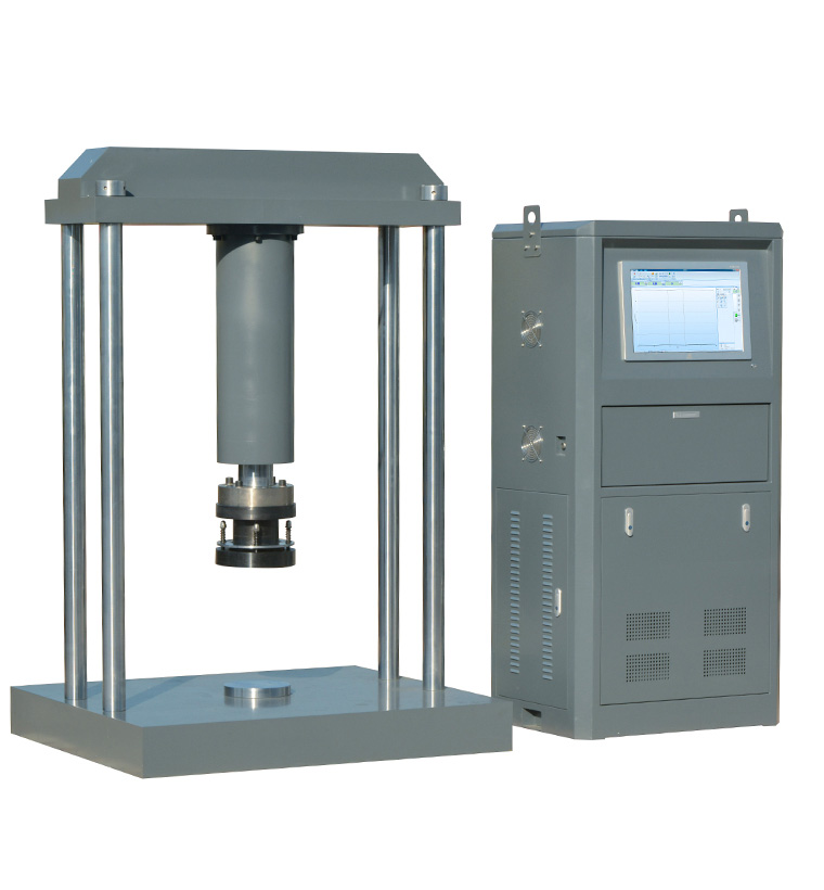
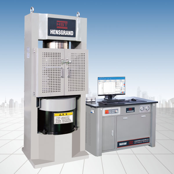
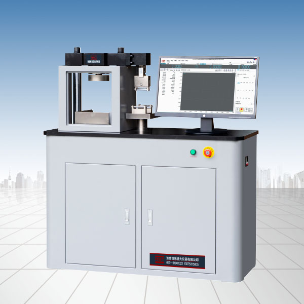
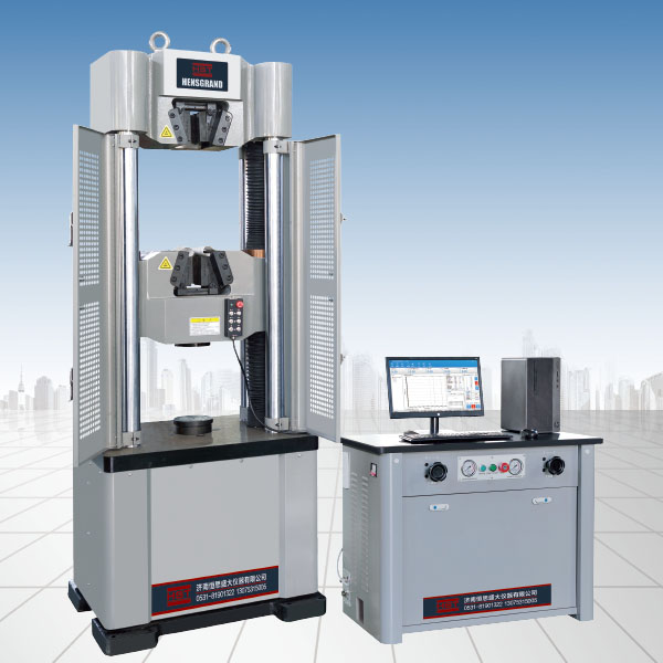
Recommended productsPRODUCTS